Building an AR488 GPIB Interface
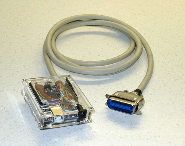
Construction of an Arduino GPIB interface is relatively straightforward and requires a single Arduino UNO, NANO or MEGA2560 board, a length of cable that is at minimum 16-way and preferably screened, and an IEEE488 connector. An old GPIB cable could be re-purposed by removing one end, or an old parallel printer cable could be used, in which case a separate 24-way IEEE488 connector will need to be purchased.
New GPIB/IEEE488 cables are expensive. Cheaper cables can be found from various sellers on eBay. Connectors can be found by searching for ‘Centronics 24’ rather than ‘IEEE488’ or ‘GPIB’. In the UK, RS Components sell these as part number 239-1207, for £2.86. They can also be found on eBay. Old parallel printer cables can still be found on charity/thrift shops or on market stalls.
For connection details and wiring diagrams for specific boards, please see:
- Appendix A – Uno and Nano
- Appendix B – Mega 2560
- Appendix C – Micro 32u4
Ideally, in a GPIB cable, ground pins 18, 19, 20, 21, 22, 23 should be connected to a
ground wire that forms a twisted pair with the DAV, NRFD, NDAC, IFC,
SRQ and ATN control wires, and a shielded twisted pair cable with sufficient
multiple pairs would be required. However, if such a cable is not available, then
linking them together and connecting them to GND on the Arduino side should suffice,
especially if sufficient numbers of conductors are not available.
Further information can be found by following the links below:
Once the cable has been completed, the sketch should then be downloaded to the Arduino board and the interface should be ready to test. In order to provide multi-platform compatibility, the AR488 firmware sketch is modular and comes in several files:
Filename:           Purpose:
AR488.ino           This is the main AR488 firmware sketch
AR488_Config.h      This is the configuration file. All configuration
                    options are set here.
AR488_Hardware.h    This is the hardware support C++ header file
AR488_Hardware.cpp  This is the hardware support C++ program file
The firmware is supplied in a ZIP file. Download and unpack all files into a directory called AR488. Load the main sketch, AR488.ino into the Arduino IDE. This should open all files into separate tabs. Edit AR488_Config.h as required and save. Then select the correct board from the list of boards within the Arduino IDE, Tools | Board menu option and compile and upload the sketch.
The following section details further hardware tweaks that may be required to make the board work correctly with specific GPIB software.
Multiple Arduinos on the bus and problems with instruments
The AR488 can be used in both controller mode and device mode and only ONE controller can be active at any one time. When there is just one Arduino controller on the bus controlling one or more instruments, this does not present a problem, provided that the Arduino is operating within its current handling limits.
However, it is possible to have one AR488 operating as a controller and another as a device simultaneously on the bus along with other instruments. In this situation and without any additional buffering (see the following section: SN7516x GPIB transceiver integrated circuits), problems can arise when two or more Arduinos are connected to the GPIB bus and one of them is powered down. Such problems are manifest by instruments failing to respond to the ++read or other commands, failing to respond to direct instrument commands, or other erratic bus communication problems.
The reason for this is because when powered down, Arduino control pins do not present with a high impedance. In a powered down state, voltages present on the various signal and data lines are passed via protection diodes internal to the ATMega processor, to the +VCC rail on the powered down interface. This then causes all pins on the unpowered Arduino to effectively go HIGH. Furthermore, enough power may be present on the +VCC rail to at least partially power the processor, which, even if it does manage to operate, is likely to do so in an unpredictable manner the result of which may be the aforementioned interference with the proper functioning of other equipment on the GPIB bus. This is a parasitic power phenomenon that is not specific to Arduino microcontrollers and that affects various other devices also. Further information regarding this phenomenon can be found here:
https://www.eevblog.com/forum/blog/eevblog-831-power-a-micro-with-no-power-pin!/
Consequently, unpowered Arduino devices will adversely affect other devices on the GPIB bus. It is therefore essential to either keep Arduino devices powered on, or physically disconnected from the bus. This is NOT an issue when there is just ONE Arduino-based GPIB controller remotely controlling instruments on a bus. Therefore, other than when an Arduino is operating as a controller, it is not recommended to leave unpowered Arduino’s connected to the bus.
SN7516x GPIB transceiver integrated circuits
The AR488 firmware supports SN75160 and SN75161 GPIB transceiver integrated circuits. These ICs provide a buffer between the Arduino and the GPIB bus and allow the full 48mA drive current for a GPIB device. In addition, when powered down, these devices present a high impedance to the GPIB bus so that the connected device does not interfere with the operation of the bus. This solves the ‘parasitic power’ problem that ocurrs when using Arduinos connected directly without buffering to the the GPIB bus and means that the interface can be safely powered down without affecting communication on the GPIB bus.
In order to use these GPIB transceiver ICs, at least one SN75160 and one SN75161 will be required and a separate daughterboard will have to be built. The SN75160 provides 3-state outputs for the data bus, whereas the SN75161 provides similar isolation for the GPIB control signals. Connection details can be found in Appendix A, which details connections for the Uno board. A similar approach can be used for any other board using available GPIO pins.
Operation of the SN75160 is simple. The Arduino outputs are connected to the ‘Terminal
I/O ports’ side of the IC and the GPIB bus DIO lines to the ‘GPIB I/O ports’ side.
The PE pin should be connected to VCC in order to provide 3-state output. The TE
(talk-enable) pin is connected to a GPIO pin on the Arduino. The GPIO pin is defined in
Config.h. For further details see the Configuration section.
The operation of the SN75161 is a little more complex as part of the IC is controlled by
the TE pin, but also by the DC (direction-control) pin. The TE pin is
connected to the same GPIO pin as the 75160 TE pin. The DC pin needs to be
driven separately. This can be achieved by connecting DC to a seperate GPIO pin
which can also be defined in Config.h. Alternatively, it can be controlled by the
REN signal. The REN signal is asserted (LOW) in controller mode and
un-asserted (HIGH) in device mode which conveniently corresponds to the drive signal
required for DC to switch between controller and device mode. When REN is being
used to control DC, it cannot be turned off as this would switch the IC into device
mode and communication would fail. For this reason, the ++ren command is not
available in this configuration (see ++ren in the Custom commands section for
details on the behaviour of this command).
The SN75162 IC differs from the SN75161 in that the REN and IFC signals are
independently controlled. The input required is the inverse of the DC signal.
Conceivably a separate GPIO pin could be used to drive the SC pin of the SN75162 but
this is currently untested and unsupported. Alternatively some means of hardware
inversion could be devised and the pin connected to DC, but in this case, experiment
at your own risk.
Arduino brownout detection setting
The first three bits of the Arduino extended fuse determine the brownout detection
(BOD) setting. BOD will hold the processor in the reset state when the power
rail voltage falls below a specific threshold. There are three threshold levels that can
be set depending on the bits that is set.
On the boards that were used for development, the default setting of the Extended
Fuse seems to be FD, which means that the last three bits will be 101 and
therefore that the BOD level is set to BODLEVEL1.
It has been reported that when BOD is disabled (e.g. fuse set to FF) and the
Arduino signal pins are connected to power, that under some circumstances the Arduino
flash memory can get corrupted and the sketch will have to be downloaded again. It is
therefore inadvisable to disable BOD on an Arduino being used as a GPIB interface.
Arduino BOD settings are as follows:
| BOD Level | Bit setting | Threshold |
|---|---|---|
| DISABLED | 111 | BOD disabled |
| BODLEVEL0 | 110 | 1.7-2.0v |
| BODLEVEL1 | 101 | 2.5-2.9v |
| BODLEVEL2 | 100 | 4.1-4.5v |
To check the extended fuse setting, the following AVRDUDE command line can be used:
UNO/NANO:
avrdude -P /dev/ttyACM0 -b 19200 -c usbasp -p m328p -v
Mega 2560:
avrdude -P /dev/ttyACM0 -b 115200 -c usbasp -p m2560 -v
MEGA 32U4:
avrdude -P /dev/ttyACM0 -b 115200 -c usbasp -p m32u4 -v
The ATMega328p part can be specified as -p m328p or -p atmega328p. The Mega 2560
and Mega 32u4 can also be specified using either convention. If your Arduino has a 328pb
processor IC, then this will have a different signature to the 328p and the -p parameter
needs to be specified as -p m328pb or -p atmega328pb.